Difference between revisions of "HFI time response model"
(Created page with '== Detection chain == <span style="color:red">(Francesco Piacentini)</span> This entire section has been moved to this page. === Bolometers=== The he…') |
(→Bolometers) |
||
| Line 3: | Line 3: | ||
This entire section has been moved to [[HFI_detection_chain | this page]]. | This entire section has been moved to [[HFI_detection_chain | this page]]. | ||
| − | |||
| − | |||
| − | |||
| − | |||
| − | |||
| − | |||
| − | |||
| − | |||
| − | |||
| − | |||
| − | |||
| − | |||
| − | |||
| − | |||
| − | |||
| − | |||
| − | |||
| − | |||
| − | |||
| − | |||
| − | |||
| − | |||
| − | |||
| − | |||
| − | |||
| − | |||
| − | |||
| − | |||
| − | |||
| − | |||
| − | |||
| − | |||
| − | |||
| − | |||
| − | |||
| − | |||
| − | |||
| − | |||
| − | |||
| − | |||
| − | |||
| − | |||
| − | |||
| − | |||
| − | |||
| − | |||
| − | |||
| − | |||
| − | |||
| − | |||
| − | |||
| − | |||
| − | |||
| − | |||
| − | |||
| − | |||
| − | |||
| − | |||
| − | |||
| − | |||
| − | |||
| − | |||
| − | |||
===Focal plane layout=== | ===Focal plane layout=== | ||
Revision as of 17:18, 30 January 2013
Contents
Detection chain[edit]
(Francesco Piacentini)
This entire section has been moved to this page.
Focal plane layout[edit]
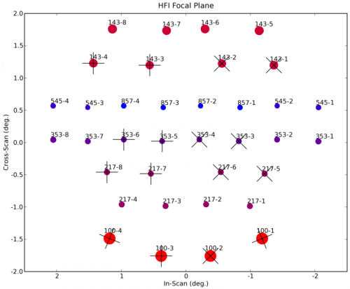
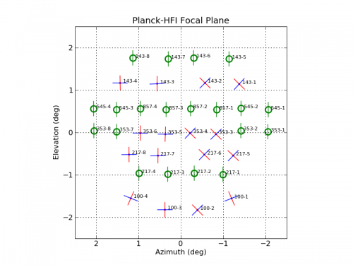
The layout of the detectors in the focal plane is defined to cope with the scanning strategy. The HFI horns are positioned at the centre of the focal plane, where the optical quality is good enough for the high frequencies. The curvature of rows compensates for the distortion of images by the telescope. A pair of identical SWB will scan the same circle on the sky to provide additional redundancy. Similar horns feeding PSBs are also aligned so that two pairs of PSBs rotated by 45◦ with respect to each other scan the same line. This will provide the Q and U Stokes parameters with minimal correction for the pointing (Rosset et al. 2010). Residual systematics will come from the differences between the beam shapes of the two horns. In all cases except for the 100 GHz horns, a measurement is also done by a pair of similar channels shifted by 1.25 arcminutes in the cross-scan direction, to ensure adequate sampling. In the figures focal plane layout is reported.

Readout[edit]
The AC bias readout electronics of the HFI instrument (Gaertner et al. 1997) includes a number of original features proposed by several laboratories (CRTBT in Grenoble, CESR in Toulouse and IAS in Orsay), which were validated on the Diabolo experiment and on the balloon-borne Archeops experiment. It was developed for space by the CESR in Toulouse.
The particular features of the HFI AC bias readout are mainly
- i)that the cold load resistors were replaced by capacitors because they have no Johnson noise;
- ii)that the detectors are biased by applying a triangular voltage to the load capacitors
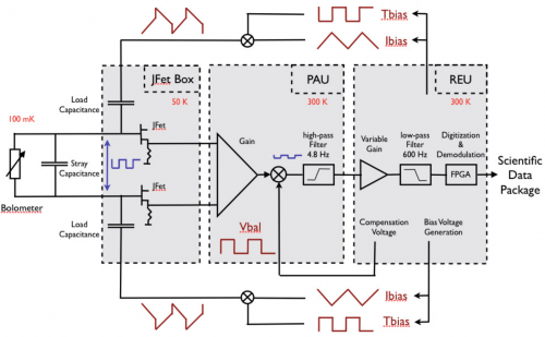
which produces a square current [Ibias ] in the capacitors, and a square voltage [T bias ] that compensates for the stray capacitance of the wiring (producing a nearly square bias current into the bolometer;
- iii)that a square offset com-pensation signal is subtracted to the bolometric signal to minimise the amplitude of the signal that has to be amplified and digitized;
- iv)that the electronic scheme is symmetrical and uses a differential amplification scheme to optimize the immunity to electromagnetic interferences;
- v)and finally that every parameter of the REU can be set by commands, which
is made possible by using digital-to-analog and analog-to-digital converters extensively.
The readout electronics consist of 72 channels designed to perform low noise measurements of the impedance of 52 bolometers, two blind bolometers, 16 accurate low temperature thermometers, all in the 10 MΩ range, one resistor of 10 MΩ and one capacitor of 100 pF. The semiconductor bolometers and thermometers of Planck-HFI operate at cryogenic temperature around 100 mK on the focal plane, with impedance of about 10 MΩ when biased at the optimal current. The readout electronics on the contrary have to operate at “room” temperature (300 K). The distance between the two extremities of the readout chain is about 10 m and could represent a point of extreme susceptibility to electromagnetic interference. The readout electronic chain was split into three boxes. These are the JFET box, located on the 50 K stage of the satellite at 2.2 m from the focal plane, the pre-amplifier unit (PAU), located 1.8m further at 300 K, and the REU, located on the opposite side of the satellite, 5 m away. Each of the three boxes (JFET, PAU and
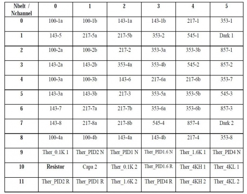
REU) consists of 12 belts of six channels. The first nine belts are dedicated to the bolometers, and the three last ones to the accurate thermometers, the resistor and the capacitor (see figure Organization of the HFI readout).
Principles of the readout electronics[edit]
See figure [Principles of readout electronics]. The bolometer is biased by a square wave AC current obtained by the differentiation of a triangular voltage through a load capacitance, in a completely differential architecture. The presence of the stray capacitance due to losses of charge in the wiring requires a correction of the shape of the square bias current by a transient voltage. Thus the bias voltage generation is controlled by the two parameters I-bias and T-bias that express the amplitude of the triangular and transient voltage. The compensation voltage added to the bolometric signal to optimize the dynamic of the chain is controlled by the V-bal parameter.
Parameters of the Readout Unit can be set to optimize the detectors performance.
The modulation frequency of the AC bias system, fmod of the square bias current can be tuned from 70 Hz to 112 Hz by the telecommand parameters: Nsample, which defines the number of samples per half period of modulated signal, fdiv which determines the sampling frequency of the ADC.
The optimal frequencies are around 90 Hz.
Each channel has its own settings for the following parameters:
I-bias, amplitude of the triangular bias voltage;
T-bias, amplitude of the transient bias voltage;
V-bal, amplitude of the square compensation voltage;
G-amp, value of the programmable gain of the REU [1/3, 1, 3, 7.6];
N-blank, number of blanked samples at the beginning of halfperiod not taken into account during integration of the signal;
S-phase, phase shift when computing the integrated signal.
All these parameters influence the effective response of the detection chains, and were optimized during the calibration campaigns and confirmed during the calibration and performance verification (CPV) phase following the launch of Planck. The scientific signal is provided by the integral of the signal on each half-period, between limits fixed by the S-phase and N-blank parameters.
The interaction of modulated readout electronics with semiconductor
bolometers is rather different from that of a classical
DC bias readout (Jones 1953). The differences were seen during
the calibration of the HFI, although the readout electronics
was designed to mimic the operation
of a DC biased bolometric system as far as possible. With the
AC readout the maximum of responsivity is lower and is obtained
for higher bias current in the bolometer with respect to the DC model.
This is caused by the stray capacitance in the
wiring which has negligible effects for a DC bias and a major
effect for an AC bias. In our case, a stray capacitance of 150 pF
induces increases of NEP ranging from 4% (857 GHz bolometers)
to 10% (100 GHz bolometers) and also affects the HFI time
response. Details of the effect of the HFI AC bias system into
the time response of the detectors are discussed in the
Time Response Section.
JFETs[edit]
Given the high impedance of the bolometers and the length of the connecting cables, it it is essential that the impedance of the signal is lowered as close as possible to the detectors. In our system this is accomplished by means of JFET source followers, located in boxes connected to the 50 K stage. The JFET box has been designed, developed and tested in the Observational Cosmology group in the Physics Department of the University of Rome "La Sapienza" (Brienza D. et al 2006). There are two JFETs per channel, since the readout is fully differential, and they provide a current amplification of the signal while keeping the voltage amplification very close to unity.
Inside the box, the JFETs are mounted on a thermally insulated plate with an active temperature control to keep them at the optimal temperature of 110 K. With a dissipated power lower than 240 mW, mainly produced by the JFETs and the source resistors, we obtained a noise power spectral density of less than 3 nV Hz1/2 for the frequency range of interest. This increases the total noise ofall bolometer channels by less than 5%.
Data compression[edit]
The output of the readout electronics unit (REU) consists of one value for each of the 72 science channels for each half-period of modulation. This number, , is the sum of the 40 16-bit ADC signal values obtained within the given half-period. The data processor unit (DPU) performs a lossy quantization of .
We define a compression slice of 254 values, corresponding to about 1.4 s of observation for each detector and to a strip of sky about 8 degrees long. The mean of the data within each compression slice is computed, and data are demodulated using this mean:
where is the running index within the compression slice.
The mean of the demodulated data is computed and subtracted, and the resulting data slice is quantized according to a step size Q that is fixed per detector:
This is the lossy part of the algorithm: the required compression factor, obtained through the tuning of the quantization step Q, adds a measure of noise to the data. Assuming Gaussian white noise with standard deviation , a quantization setting of /Q = 2 adds 1% to the noise (Pajot et al. 2010; Pratt 1978). The value of was determined at the end of the CPV phase after subtraction of the signal from the timeline.
The two means and are computed as 32-bit words and sent through the telemetry, together with the values. Variable-length encoding of the values is performed on board, and the inverse decoding is applied on ground.
Optimal use of the bandpass available for the downlink (75 kb/s
average for HFI science) was obtained initially by using a value
of Q = /2.5 for all bolometer signals.
After 12 December 2009, only for the 857 GHz detectors, the
value was reset to Q = /2.0 to avoid data loss
due to exceeding the limit of downlink rate.
Time response[edit]
The HFI bolometers and readout electronics have a finite response time to changes in incident optical power. The bolometers are thermal detectors of radiation whose response time is determined by the thermal circuit defined by the heat capacity of the detector and thermal conductivity.
Due to Planck's nearly constant scan rate, the time response is degenerate with the optical beam. However, because of the long time scale effects present in the time response, the time response is deconvolved from the data in the processing of the HFI data (see TOI processing).
The time response of the HFI bolometers and readout electronics is modeled as a Fourier domain transfer function (called the LFER4 model) consisting of the product of an bolometer thermal response and an electronics response .
LFER4 model[edit]
If we write the input signal (power) on a bolometer as the bolometer physical impedance can be written as: where is the angular frequency of the signal and is the complex intrinsic bolometer transfer function. For HFI the bolometer transfer function is modelled as the sum of 4 single pole low pass filters: The modulation of the signal is done with a square wave, written here as a composition of sine waves of decreasing amplitude: where we have used the Euler relation and is the angular frequency of the square wave. The modulation frequency is and was set to Hz in flight. This signal is then filtered by the complex electronic transfer function . Setting: we have: This signal is then sampled at high frequency (). is one of the parameters of the HFI electronics and corresponds to the number of high frequency samples in each modulation semi-period. In order to obtain an output signal sampled every seconds, we must integrate on a semiperiod, as done in the HFI readout. To also include a time shift , the integral is calculated between and (with period of the modulation). The time shift is encoded in the HFI electronics by the parameter , with the relation .
After integration, the -sample of a bolometer can be written as where
The output signal in equation eqn:output can be demodulated (thus removing the ) and compared to the input signal in equation bol_in. The overall transfer function is composed of the bolometer transfer function and the effective electronics transfer function, :
The shape of is obtained combining low and high-pass filters with Sallen Key topologies (with their respective time constants) and accounting also for the stray capacitance low pass filter given by the bolometer impedance combined with the stray capacitance of the cables. The sequence of filters that define the electronic band-pass function are listed in table table:readout_electronics_filters.
Parameters of LFER4 model[edit]
The LFER4 model has are a total of 10 parameters(,,,,,,,,,) 9 of which are independent, for each bolometer. The free parameters of the LFER4 model are determined using in-flight data in the following ways:
- is fixed at the value of the REU setting.
- is measured during the QEC test during CPV.
- , , , are fit forcing the compactness of the scanning beam.
- , , are fit by forcing agreement of survey 2 and survey 1 maps.
- The overall normalization of the LFER4 model is forced to be 1.0 at the signal frequency of the dipole.
The details of determining the model parameters are given in (reference P03c paper) and the best-fit parameters listed here in table table:LFER4pars.
HFI electronics filter sequence[edit]
| Filter | Parameters | Function |
|---|---|---|
| 0. Stray capacitance low pass filter | ||
| 1. Low pass filter | k nF |
|
| 2. Sallen Key high pass filter | k |
3 |
| 3. Sign reverse with gain | ||
| 4. Single pole low pass filter with gain | k nF |
|
| 5. Single pole high pass filter coupled to a Sallen Key low pass filter | k k nF k F |
| Bolometer | (s) | (s) | (s) | (s) | (s) | (s) | ||||
| 100-1a | 0.392 | 0.01 | 0.534 | 0.0209 | 0.0656 | 0.0513 | 0.00833 | 0.572 | 0.00159 | 0.00139 |
| 100-1b | 0.484 | 0.0103 | 0.463 | 0.0192 | 0.0451 | 0.0714 | 0.00808 | 0.594 | 0.00149 | 0.00139 |
| 100-2a | 0.474 | 0.00684 | 0.421 | 0.0136 | 0.0942 | 0.0376 | 0.0106 | 0.346 | 0.00132 | 0.00125 |
| 100-2b | 0.126 | 0.00584 | 0.717 | 0.0151 | 0.142 | 0.0351 | 0.0145 | 0.293 | 0.00138 | 0.00125 |
| 100-3a | 0.744 | 0.00539 | 0.223 | 0.0147 | 0.0262 | 0.0586 | 0.00636 | 0.907 | 0.00142 | 0.00125 |
| 100-3b | 0.608 | 0.00548 | 0.352 | 0.0155 | 0.0321 | 0.0636 | 0.00821 | 0.504 | 0.00166 | 0.00125 |
| 100-4a | 0.411 | 0.0082 | 0.514 | 0.0178 | 0.0581 | 0.0579 | 0.0168 | 0.37 | 0.00125 | 0.00125 |
| 100-4b | 0.687 | 0.0113 | 0.282 | 0.0243 | 0.0218 | 0.062 | 0.00875 | 0.431 | 0.00138 | 0.00139 |
| 143-1a | 0.817 | 0.00447 | 0.144 | 0.0121 | 0.0293 | 0.0387 | 0.0101 | 0.472 | 0.00142 | 0.00125 |
| 143-1b | 0.49 | 0.00472 | 0.333 | 0.0156 | 0.134 | 0.0481 | 0.0435 | 0.27 | 0.00149 | 0.00125 |
| 143-2a | 0.909 | 0.0047 | 0.0763 | 0.017 | 0.00634 | 0.1 | 0.00871 | 0.363 | 0.00148 | 0.00125 |
| 143-2b | 0.912 | 0.00524 | 0.0509 | 0.0167 | 0.0244 | 0.0265 | 0.0123 | 0.295 | 0.00146 | 0.00125 |
| 143-3a | 0.681 | 0.00419 | 0.273 | 0.00956 | 0.0345 | 0.0348 | 0.0115 | 0.317 | 0.00145 | 0.00125 |
| 143-3b | 0.82 | 0.00448 | 0.131 | 0.0132 | 0.0354 | 0.0351 | 0.0133 | 0.283 | 0.00161 | 0.000832 |
| 143-4a | 0.914 | 0.00569 | 0.072 | 0.0189 | 0.00602 | 0.0482 | 0.00756 | 0.225 | 0.00159 | 0.00125 |
| 143-4b | 0.428 | 0.00606 | 0.508 | 0.00606 | 0.0554 | 0.0227 | 0.00882 | 0.084 | 0.00182 | 0.00125 |
| 143-5 | 0.491 | 0.00664 | 0.397 | 0.00664 | 0.0962 | 0.0264 | 0.0156 | 0.336 | 0.00202 | 0.00139 |
| 143-6 | 0.518 | 0.00551 | 0.409 | 0.00551 | 0.0614 | 0.0266 | 0.0116 | 0.314 | 0.00153 | 0.00111 |
| 143-7 | 0.414 | 0.00543 | 0.562 | 0.00543 | 0.0185 | 0.0449 | 0.00545 | 0.314 | 0.00186 | 0.00139 |
| 217-5a | 0.905 | 0.00669 | 0.0797 | 0.0216 | 0.00585 | 0.0658 | 0.00986 | 0.342 | 0.00157 | 0.00111 |
| 217-5b | 0.925 | 0.00576 | 0.061 | 0.018 | 0.00513 | 0.0656 | 0.0094 | 0.287 | 0.00187 | 0.00125 |
| 217-6a | 0.844 | 0.00645 | 0.0675 | 0.0197 | 0.0737 | 0.0316 | 0.0147 | 0.297 | 0.00154 | 0.00125 |
| 217-6b | 0.284 | 0.00623 | 0.666 | 0.00623 | 0.0384 | 0.024 | 0.0117 | 0.15 | 0.00146 | 0.00111 |
| 217-7a | 0.343 | 0.00548 | 0.574 | 0.00548 | 0.0717 | 0.023 | 0.0107 | 0.32 | 0.00152 | 0.00139 |
| 217-7b | 0.846 | 0.00507 | 0.127 | 0.0144 | 0.0131 | 0.0479 | 0.0133 | 0.311 | 0.00151 | 0.00139 |
| 217-8a | 0.496 | 0.00722 | 0.439 | 0.00722 | 0.0521 | 0.0325 | 0.0128 | 0.382 | 0.00179 | 0.00111 |
| 217-8b | 0.512 | 0.00703 | 0.41 | 0.00703 | 0.0639 | 0.0272 | 0.0139 | 0.232 | 0.00173 | 0.00125 |
| 217-1 | 0.0136 | 0.00346 | 0.956 | 0.00346 | 0.0271 | 0.0233 | 0.00359 | 1.98 | 0.00159 | 0.00111 |
| 217-2 | 0.978 | 0.00352 | 0.014 | 0.0261 | 0.00614 | 0.042 | 0.00194 | 0.686 | 0.0016 | 0.00125 |
| 217-3 | 0.932 | 0.00355 | 0.0336 | 0.00355 | 0.0292 | 0.0324 | 0.00491 | 0.279 | 0.00174 | 0.00125 |
| 217-4 | 0.658 | 0.00135 | 0.32 | 0.00555 | 0.0174 | 0.0268 | 0.00424 | 0.473 | 0.00171 | 0.00111 |
| 353-3a | 0.554 | 0.00704 | 0.36 | 0.00704 | 0.0699 | 0.0305 | 0.0163 | 0.344 | 0.0017 | 0.00125 |
| 353-3b | 0.219 | 0.00268 | 0.671 | 0.00695 | 0.0977 | 0.0238 | 0.0119 | 0.289 | 0.00157 | 0.00111 |
| 353-4a | 0.768 | 0.00473 | 0.198 | 0.00993 | 0.0283 | 0.0505 | 0.00628 | 0.536 | 0.00181 | 0.00125 |
| 353-4b | 0.684 | 0.00454 | 0.224 | 0.0108 | 0.0774 | 0.08 | 0.0149 | 0.267 | 0.00166 | 0.00111 |
| 353-5a | 0.767 | 0.00596 | 0.159 | 0.0124 | 0.0628 | 0.0303 | 0.0109 | 0.357 | 0.00156 | 0.00111 |
| 353-5b | 0.832 | 0.00619 | 0.126 | 0.0111 | 0.0324 | 0.035 | 0.0096 | 0.397 | 0.00166 | 0.00111 |
| 353-6a | 0.0487 | 0.00176 | 0.855 | 0.006 | 0.0856 | 0.0216 | 0.0105 | 0.222 | 0.00199 | 0.00125 |
| 353-6b | 0.829 | 0.00561 | 0.127 | 0.00561 | 0.0373 | 0.0252 | 0.00696 | 0.36 | 0.00228 | 0.00111 |
| 353-1 | 0.41 | 0.000743 | 0.502 | 0.00422 | 0.0811 | 0.0177 | 0.0063 | 0.329 | 0.00132 | 0.00097 |
| 353-2 | 0.747 | 0.00309 | 0.225 | 0.00726 | 0.0252 | 0.0447 | 0.00267 | 0.513 | 0.00154 | 0.00097 |
| 353-7 | 0.448 | 0.0009 | 0.537 | 0.0041 | 0.0122 | 0.0273 | 0.00346 | 0.433 | 0.00178 | 0.00125 |
| 353-8 | 0.718 | 0.00223 | 0.261 | 0.00608 | 0.0165 | 0.038 | 0.00408 | 0.268 | 0.00177 | 0.00111 |
| 545-1 | 0.991 | 0.00293 | 0.00743 | 0.026 | 0.00139 | 2.6 | 0 | 0 | 0.00216 | 0.00111 |
| 545-2 | 0.985 | 0.00277 | 0.0128 | 0.024 | 0.00246 | 2.8 | 0 | 0 | 0.00187 | 0.00097 |
| 545-4 | 0.972 | 0.003 | 0.0277 | 0.025 | 0.000777 | 2.5 | 0 | 0 | 0.00222 | 0.00111 |
| 857-1 | 0.974 | 0.00338 | 0.0229 | 0.025 | 0.00349 | 2.2 | 0 | 0 | 0.00176 | 0.00111 |
| 857-2 | 0.84 | 0.00148 | 0.158 | 0.00656 | 0.00249 | 3.2 | 0 | 0 | 0.0022 | 0.00125 |
| 857-3 | 0.36 | 4.22e-05 | 0.627 | 0.0024 | 0.0111 | 0.017 | 0.002 | 1.9 | 0.00152 | 0.00126 |
| 857-4 | 0.278 | 0.0004 | 0.719 | 0.00392 | 0.00162 | 0.09 | 0.00152 | 0.8 | 0.00149 | 0.000558 |
(Planck) High Frequency Instrument
Readout Electronic Unit
Junction Field Elect Transistor
Pre_Amplification Unit
analog to digital converter
Calibration and Performance Verification
Noise Equivalent Power
Data Processing Unit


